Advanced Characterization
The observation of some nanoelectronic phenomena (in a reliable manner) is a very complex task that requires the combination of multiple machines
and also adjusting them in non-standard sophisticated ways. In our laboratory, we have wide experience in these types of experiments, which helped us to clarify multiple behaviours about our samples. For example, our group has developed multiple improvements
to standard conductive atomic force microscopes, such as connecting a semiconductor parameter analyser directly to the tip of the conductive atomic force microscope (CAFM). This allowed us to observe with unprecedented clarity the dynamics of the
dielectric breakdown [1-2] and resistive switching [3-4] in situ, and, more recently, we reported the first observation of electro-synaptic response at the nanoscale using the tip of the CAFM [5]. In some cases, these experiments required us to develop
environmental chambers [6] or to clarify complex phenomena related to the effect of the laser on optoelectronic samples [7]. We also developed a method to stress materials using ionic liquid, so that later the surface of the sample can be scanned
via CAFM without having to remove a solid metallic electrode (which damages the surface) [8]. We collaborate with multiple world-leading scientists, who send us their samples for characterization, including Prof. Paul McIntyre from Stanford University
[9], Prof. Jing Kong from Massachusetts Institute of Technology [10], and Prof. Andrea Ferrari from University of Cambridge [5], among many others.
Since we arrived to KAUST we have been offering advanced characterization of all kinds
of materials using the state-of-the-art nano-characterization facilities of the university. For example, our trained students have carried out cross-sectional transmission electron microscopy (TEM) for top scientists like Prof. Barbaros Oezylmaz from National University
of Singapore, Prof. Tibor Grasser from TU Wien [11] and Prof. Tania Roy from Duke University [12]. An example of a top-view TEM image with atomic resolution collected in our laboratories at KAUST can be seen in Figure 1. We always complement the cross-sectional
TEM images of the samples with atomic-scale chemical characterization using energy dispersive X-ray spectroscopy (EDS) and electron energy loss spectroscopy (EELS) [13], although at KAUST we have many other cutting-edge machines for advanced characterization.
A complete list of the facilities from KAUST can be found here.
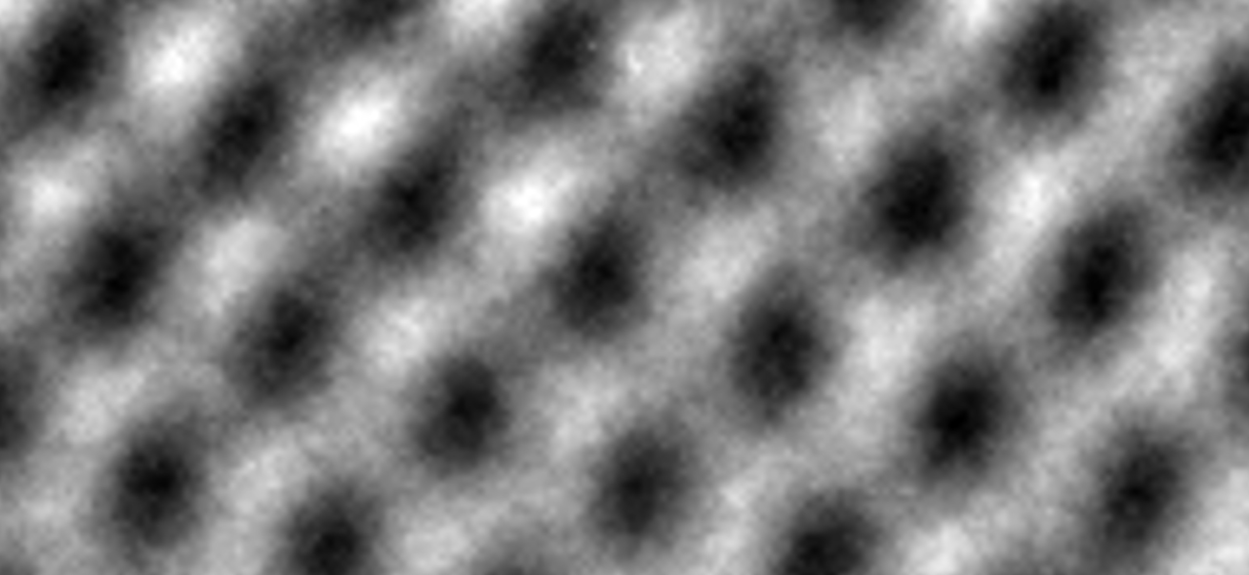
Figure 1: Top-view transmission electron microscopy of a nanoparticle with atomic-scale resolution. The atoms are seen as black regions and the distance between them is 0.3 nm.
References
[1] Fei Hui, Pujashree Vajha, Yuanyuan Shi, Yanfeng Ji, Huiling Duan, Andrea Padovani, Luca Larcher, Xiao-Rong Li, Jing-Juan Xu, Mario Lanza*, Moving graphene
devices from lab to market: advanced graphene-coated nanoprobes, Nanoscale, 8, 8466–8473, 2016
[2] M. Lanza, M. Porti, M. Nafría, X. Aymerich, G. Benstetter, E. Lodermeier, H. Ranzinger G. Jaschke, S. Teichert, L. Wilde and P. Michalowski,
Conductivity and charge trapping after electrical stress in amorphous and polycristalline Al2O3 based devices studied with AFM related techniques, IEEE Transactions on Nanotechnology, 10 (2), 344-351, 2011.
[3] M. Lanza*, G. Bersuker, M. Porti,
E. Miranda, M. Nafría, X. Aymerich, Resistive switching in hafnium dioxide layers: Local phenomenon at grain boundaries, Applied Physics Letters vol. 101, Art. No. 193502, 2012.
[4] M. Lanza*, K. Zhang, M. Porti, M. Nafria, Z. Y. Shen*,
L. F. Liu*, J. F. Kang, D. Gilmer, and G. Bersuker, Grain boundaries as preferential sites for resistive switching in the HfO2 resistive random access memory structures, Applied Physics Letters 100, 123508, 2012.
[5] Fei Hui, Peisong Liu, Stephen
A Hodge, Tian Carey, Chao Wen, Felice Torrisi, D Thanuja L Galhena, Flavia Tomarchio, Yue Lin, Enrique Moreno, Juan B Roldan, Elad Koren, Andrea C Ferrari, Mario Lanza*. In Situ Observation of Low-Power Nano-Synaptic Response in Graphene Oxide Using
Conductive Atomic Force Microscopy. Small. 2021, 17, 2101100.
[6] Yanfeng Ji, Fei Hui, Yuanyuan Shi, Tingting Han, Xiaoxue Song, Chengbin Pan and Mario Lanza*, Fabrication of a fast-response and user-friendly environmental chamber for atomic
force microscopes, Review of Scientific Instruments, 86, 106105, 2015.
[7] Yanfeng Ji, Fei Hui, Yuanyuan Shi, Vanessa Iglesias, David Lewis, Jiebin Niu, Shibing Long, Ming Liu, Alexander Hofer, Werner Frammelsberger, Guenther Benstetter, Andrew
Scheuermann, Paul C. McIntyre, Mario Lanza*, Characterization of the photocurrents generated by the laser of atomic force microscopes, Review of Scientific Instruments, 87, 083703, 2016.
[8] Mario Lanza*, Kechao Tang, Andrew C. Meng, Fei Hui,
Yuanyuan Shi, Tingting Han, Trevor Petach, Charles Hitzman, Ai Leen Koh, David Goldhaber-Gordon, Paul C. McIntyre, “Using Liquid Electrolytes in Dielectric Reliability Studies”, 24th IEEE International Symposium on the Physical and Failure
Analysis of Integrated Circuits (IEEE-IPFA), July 16th-19th 2018, Singapore. DOI: 10.1109/IPFA. 2018.8452552.
[9] Kechao Tang, Andrew C. Meng, Fei Hui, Yuanyuan Shi, Trevor Petach, Charles Hitzman, Ai Leen Koh, David Goldhaber-Gordon, Mario Lanza,
and Paul C. McIntyre*, Distinguishing Oxygen Vacancy Electromigration and Conductive Filament Formation in TiO2 Resistance Switching Using Liquid Electrolyte Contacts, Nano Letters, 17 (7), 4390–4399, 2017.
[10] Fei Hui, Wenjing Fang, Wei
Sun Leong, Tewa Kpulun, Haozhe Wang, Hui Ying Yang, Gary Harris, Jing Kong, Mario Lanza*, Electrical homogeneity of chemical vapor deposited hexagonal boron nitride, ACS Applied Materials & Interfaces 9 (46), 39895-39900, 2017.
[11] Chao
Wen, Alexander G. Banshchikov, Yury Y. Illarionov, Werner Frammelsberger, Theresia Knobloch, Fei Hui, Nikolai S. Sokolov, Tibor Grasser, Mario Lanza*, Dielectric Properties of Ultrathin CaF2 Ionic Crystals, Advanced Materials, 32 (34), 2002525, 2020.
[12] Adithi Krishnaprasad, Durjoy Dev, Sang Sub Han, Yaqing Shen, Hee-Suk Chung, Tae-Sung Bae, Changhyeon Yoo, Yeonwoong Jung, Mario Lanza, and Tania Roy. MoS2 Synapses with Ultra-low Variability and Their Implementation in Boolean Logic, ACS Nano
2022, 16, 2, 2866–2876.
[13] Wenwen Zheng, Fernan Saiz, Yaqing Shen, Kaichen Zhu, Yingwen Liu, Clifford McAleese, Ben Conran, Xiaochen Wang, Mario Lanza*. Defect-Free Metal Deposition on 2D Materials via Inkjet Printing Technology. Advanced
Materials 2021, 2104138.