Memristive Technologies
Memristive devices exhibit an electrical resistance that can be adjusted to two or more non-volatile levels by applying electrical stresses. [1] The core of the most advanced memristive devices is a metal/insulator/metal nanocell made of phase-change,
metal-oxide, magnetic or ferroelectric materials, which is often placed in series with other circuital elements (resistor, selector, transistor) to enhance their performance in array configurations (avoid damage during state transition, minimize intercell
disturbance) [2]. Memristive effect was discovered in 1969 [3] and the first commercial product appeared in 2006, which consisted on a 4-megabit non-volatile memory based on magnetic materials [4]. In the past few years the switching endurance, data
retention time, energy consumption, switching time, integration density, and price of memristive non-volatile memories has been remarkably improved (depending on the materials employed, values up to ~1015 cycles, >10 years, ~0.1 pJ,
~10 ns, 256 Gigabit/die and ≤0.3 $/Gigabit have been achieved) [5].
As of 2021, memristive memories are being employed as both standalone memory and embedded in application-specific integrated circuits for the internet-of-things (smart
watches and glasses, medical equipment, computers), and their market value exceeds $621 million [6]. Recent studies have shown that memristive devices may also be exploited for advanced computation, data security and mobile communication (see Figure
1) [2]. Advanced computation refers to the hardware implementation of artificial neural networks by exploiting memristive attributes like progressive conductance increase and decrease, vector matrix multiplication (in crossbar arrays) and spike-timing
dependent plasticity; state-of-the-art developments have achieved >10 trillions of operations per second per watt [7-8]. Data encryption can be realized by exploiting the stochasticity inherent to the memristive effect, which is manifested as random
fluctuations (within a given range) of the switching voltages/times and state currents. For example, true random number generators and physical unclonable functions produce random codes when exposing a population of memristive devices to an electrical
stress at 50% of switching probability (it is impossible to predict which devices will switch because that depends on their atomic structure) [9-10]. Mobile communication can also benefit from memristive devices because they could be employed as 5G
and terahertz switches with low energy consumption owing to the non-volatile nature of the resistive states —the current commercial technology is based on silicon transistors, but they are volatile and consume data both during switching and
when idle periods. State-of-the-art developments achieved cut-off frequencies >100 Terahertz with excellent insertion loss and isolation [11-12].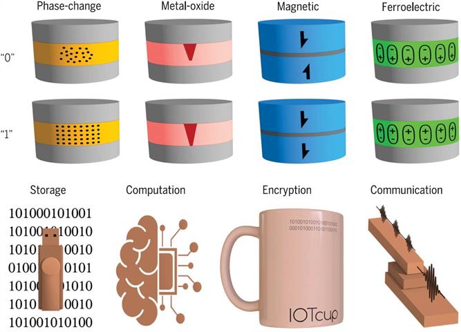
Figure 1: Fundamental memristive effects and their applications. Memristive devices, in which electrical resistance can be adjusted to two or more nonvolatile levels, can be fabricated using different materials (top row). This allows adjusting their performance to fulfill the requirements of different technologies. Memristive memories are a reality, and important progress is being achieved in advanced computation, security systems, and mobile communication (bottom row).
In this context, our group has contributed to the fabrication of memristive devices and circuits for different applications. The most innovative point of our memristive devices is the integration of multilayer hexagonal boron nitride (h-BN)
as an insulator between the two electrodes, which does the devices with special properties. More specifically, we have reported the first use of memristive h-BN devices as electronic memory [13-14], which exhibited non-volatile bipolar resistive switching.
We also observed that h-BN memristive devices could be used as electronic synapses and electronic neurons for the hardware implementation of artificial neural networks [15-16]. More recently, we also used h-BN memristors as an entropy source for true
random number generators and observed that this behaviour is quite stable due to the confinement effect of electron transport across the native defects of the h-BN grown by chemical vapour deposition [17]. We also have written some reviews articles
[2], as well as methods articles [1, 18] to clarify how to obtain the main figures-of-merit of these devices.
References
[1] Mario Lanza,* et al. Recommended
Methods to Study Resistive Switching Devices, Advanced Electronic Materials, 1800143, 2018.
[2] Mario Lanza*, Abu Sebastian, Wei D. Lu, Manuel Le Gallo, Meng-Fan Chang, Deji Akinwande, Francesco M. Puglisi, Husam N. Alshareef, Ming Liu, Juan
B. Roldan. Memristive technologies for data storage, computation, encryption, and radio-frequency communication. Science, 2022, 376, eabj9979.
[3] C.H. Sie, Memory cell using bistable resistivity in amorphous As-Te-Ge film. Iowa State University.
3604 (1969). doi.org: 10.31274/rtd-180813-1655
[4] David Lammers, MRAM debut cues memory transition, EE Times, October 7, 2006. <https://www.eetimes.com/mram-debut-cues-memory-transition/>
[5] The international roadmap for devices
and systems (2020). <https://irds.ieee.org/>
[6] Emerging non-volatile memory 2021 (market analysis report), Yole Development, https://www.i-micronews.com/products/emerging-non-volatile-memory-2021/>
[13] Francesco Puglisi*, Luca
Larcher, Chengbin Pan, Fei Hui, Na Xiao, Yanfeng Ji, Mario Lanza*, 2D h-BN based RRAM, IEEE International Electron Device Meeting (IEEE-IEDM), Dec. 4th-7th 2016, San Francisco, USA. DOI: 10.1109/IEDM.2016.7838544.
[14] Chengbin Pan, Enrique Miranda,
Marco A. Villena, Na Xiao, Xu Jing, Xiaoming Xie, Tianru Wu, Fei Hui, Yuanyuan Shi, Mario Lanza*, Model for multi-filamentary conduction in graphene/hexagonal-boron-nitride/graphene based resistive switching devices, 2D Materials, 4, 025099, 2017.
[15] Yuanyuan Shi, Xianhu Liang, Bin Yuan, Victoria Chen, Haitong Li, Fei Hui, Zhouchangwan Yu, Fang Yuan, Eric Pop, H.-S. Philip Wong, Mario Lanza*, Electronic synapses made of layered two-dimensional materials, Nature Electronics 1,
458–465, 2018.
[16] Shaochuan Chen, Mohammad Reza Mahmoodi, Yuanyuan Shi, Chandreswar Mahata, Bin Yuan, Xianhu Liang, Chao Wen, Fei Hui, Deji Akinwande, Dmitri B. Strukov, Mario Lanza*, Wafer-scale integration of 2D materials in high-density
memristive crossbar arrays for artificial neural networks, Nature Electronics, 3, 638-645, 2020
[17] Chao Wen, Xuehua Li, Tommaso Zanotti, Francesco M. Puglisi, Yuanyuan Shi, Fernan Saiz, Aleandro Antidormi, Stephan Roche, Wenwen Zheng, Xianhu
Liang, Jiaxin Hu, Steffen Duhm, Juan B. Roldan, Tianru Wu, Victoria Chen, Eric Pop, Blas Garrido, Kaichen Zhu, Fei Hui, Mario Lanza*, Advanced data encryption using two-dimensional materials, Advanced Materials 2021, 33 (27), 2100185.
[18] Mario
Lanza*, Rainer Waser, Daniele Ielmini, J Joshua Yang, Ludovic Goux, Jordi Suñe, Anthony Joseph Kenyon, Adnan Mehonic, Sabina Spiga, Vikas Rana, Stefan Wiefels, Stephan Menzel, Ilia Valov, Marco A Villena, Enrique Miranda, Xu Jing, Francesca
Campabadal, Mireia B Gonzalez, Fernando Aguirre, Felix Palumbo, Kaichen Zhu, Juan Bautista Roldan, Francesco Maria Puglisi, Luca Larcher, Tuo-Hung Hou, Themis Prodromakis, Yuchao Yang, Peng Huang, Tianqing Wan, Yang Chai, Kin Leong Pey, Nagarajan
Raghavan, Salvador Dueñas, Tao Wang, Qiangfei Xia, Sebastian Pazos. Standards for the characterization of endurance in resistive switching devices. ACS Nano. 2021, 15, 11, 17214–17231.