Lanza laboratory
Our laboratory is located in Building 3, room 2710. It consists of a rectangular room with an area of 200 square meters, and it contains four fume hoods and one smaller room. Three of the fume hoods will host a chemical vapour deposition (CVD) tube furnace of 3 inches in diameter, for the synthesis of graphene, hexagonal boron nitride, and molybdenum disulfide on 2-inch wafers (from Planartech). So far, the CVD system for synthesis of hexagonal boron nitride has been installed and is running, the other two will be installed soon. Each CVD system is exclusively dedicated to a single material to avoid cross-contamination. We also have one stage doted with an optical microscope and a rotating platform for mechanical exfoliation, transfer, and alignment of 2D materials (from HQ Graphene). Moreover, we also have an additional optical microscope (from Leica) with a much higher resolution that can measure in reflexion and transmission modes. The big room is completed with two probe stations (from Form Factor), each of them connected to a semiconductor parameter analyser (from Keysight). All the equipment is brand new and is being maintained periodically by the expert team of scientists from the Core Labs of KAUST.
In the small room, we have the atomic force microscope (AFM), a new Dimension Icon from Bruker. This system has been customized by Prof. Mario Lanza, and includes all kinds of accessories for advanced electronic, mechanical, and thermal characterization at the nanoscale. In particular, we got the conductive atomic force microscopy (CAFM) module for electrical measurements in contact mode, which comes with a current limitation function to prevent tips from damaging. In this sense, we can also use the peak force TUNA module for electro-mechanical characterization in tapping mode, which preserves the tips by removing lateral frictions. We also got the scanning thermal microscopy module that allows us to apply and measure temperature locally, as well to analyse the thermal heat generated in our devices in operando. All this is completed with a nitrogen chamber for temperatures in low humidity (down to 0.1%), a thermal stage for temperatures ranging from -60 to 150 ºC, and a piezo-stage to analyse the materials under biaxial compressive and tensile stresses up to 20 kN. Additionally, we also have a semiconductor parameter analyser that can be connected directly to the tip of the AFM to apply fast pulses, allowing us to measure complex phenomena such as electro-synaptic plasticity (among others).
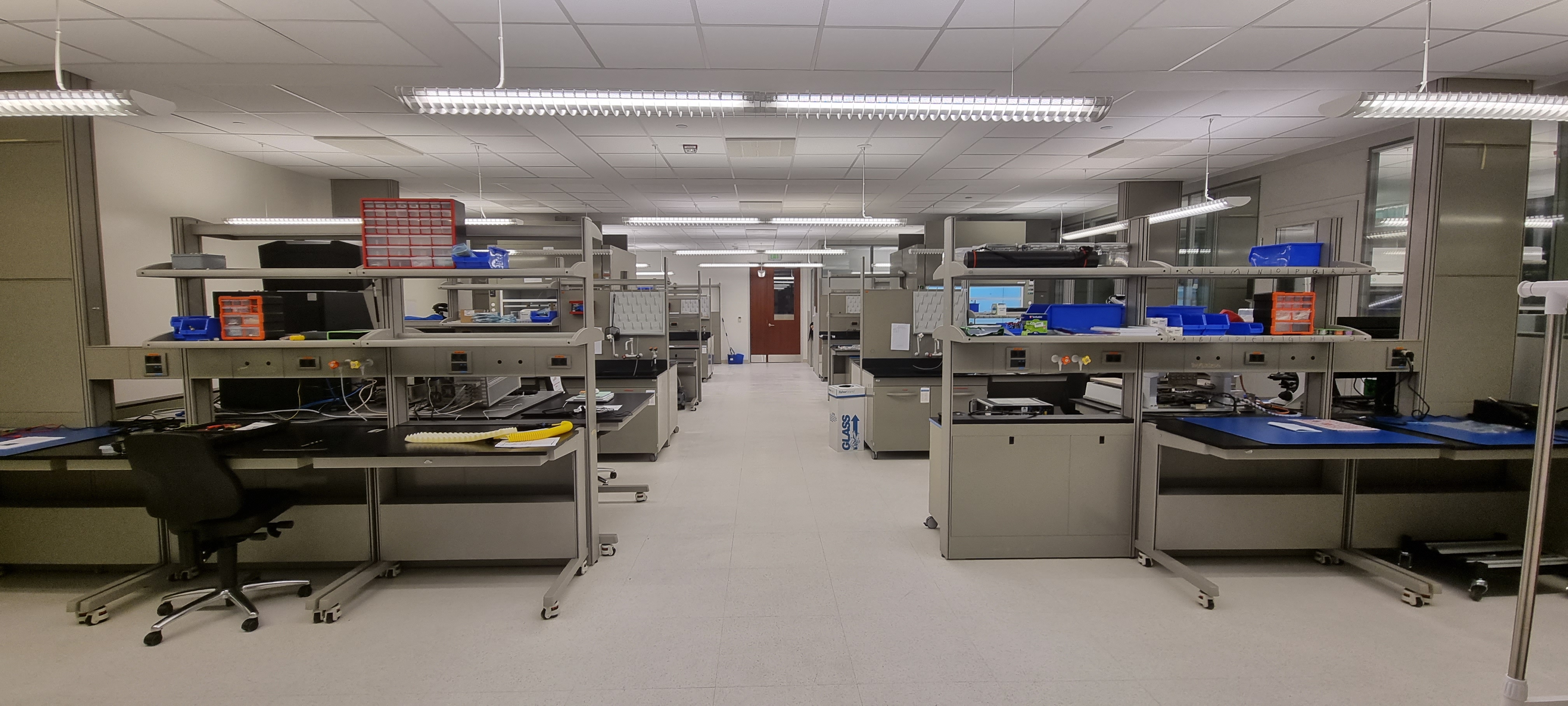
Figure 1: Private laboratory of professor Mario Lanza at KAUST, which is devoted to disruptive electronic characterization of nanomaterials, devices and circuits.