Hybrid 2D/CMOS microchips
Two-dimensional (2D) layered materials may spawn a revolution in the field of solid-state micro/nano-electronic devices and circuits, owing to their outstanding electronic, physical, chemical, and thermal properties [1]. Some top scientists and companies suggested that 2D materials could be used to mitigate the limitations of silicon technologies, help to extend the Moore’s Law, and create new concept devices beyond the complementary metal-oxide-semiconductor (CMOS) technology [2]. Top microchip manufacturers like TSMC, Samsung, Intel, and IBM and semiconductor research institutes like IMEC have already reported prototype field-effect transistors with 2D semiconducting channels [3-4]. The International Roadmap for Devices and Systems (IRDS) — a document written by a world-class group of industry-led experts (who foreshadowed important developments in the past) — lists 2D materials as an option for commercial transistors and other beyond-CMOS devices around 2028 [5] (see Figure 1).
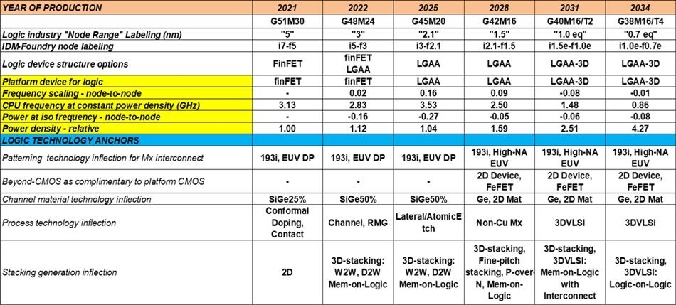
Figure 1: Table from the 2021 edition of the IRDS in which, for the first time, 2D materials were proposed as a potential solution for “Channel material technology inflection” and “Beyond CMOS as complimentary to mainstream CMOS” by 2028. Reproduced with permission from reference [5], copyright IEEE 2021.
The current status is: electronic devices made of 2D materials produced by mechanical exfoliation of small crystals have exhibited outstanding performance, such as transistors with 2D semiconducting channels that achieve high mobility (700cm2/Vs),
high current on/off ratio (>105) and low subthreshold swing (74mV/decade) [6]. However, when nanosized devices (area <0.1µm2) are produced using scalable fabrication techniques, such as chemical vapour deposition (CVD), the performance
remarkably degrades. For example, some of the best 2D-materials-based nanosized transistors (channel area ~0.0075µm2) fabricated by the industry show low mobility ~20cm2/Vs and high subthreshold swing ~134mV/decade [7], with very high device-to-device
variability. The reason is the presence of local defects in the 2D materials and contamination [8]. Interestingly enough, 2D materials show the promise for lower variability compared to silicon technology because of the amazing electrostatic control
associated with these very thin channels [9].
By now, we have seen that 2D materials have started to be integrated in some commercial products that do not require a high integration density, such as sensors [10] and specialty cameras [11] — in these bigger devices the effect of local defects in the 2D material is not so detrimental. However, commercial high-integration-density electronic circuits exploiting the properties of 2D materials are still a matter of research. Hopefully, as 2D materials start to enter in industrial laboratories with more controlled environments and materials processing (lithography, etching, deposition), the density of local defects and contamination can be reduced and ultra-scaled devices might exhibit better performance and reliability.
In the past few years, our group has made major contributions in this field. We have focused in hexagonal boron nitride (h-BN), a 2D material of strategic importance because it has one of the widest band gaps,
which enables its use as dielectric in electronic devices. More specifically, we have clarified how electrical charges flow across it (i.e., out of plane) [12-13], what is its electrical homogeneity, variability, and reliability [14-16], and how is
it affected when depositing metals on it (via evaporation and inkjet printing) [17]. We have also used this material to fabricate different electronic devices, such as transistors and memristors [18-19]. We have also studied other 2D insulators, such
as CaF2 [20-21] and graphene oxide [22-23]. We have also written some review articles to explain the community how 2D materials should be employed and their limitations [24-25].
References
[1] Backes, C. et al. Production and processing of graphene and related materials. 2D Mater. 7, 022001 (2020).
[2] Li, M.-Y. et al. How 2D semiconductors could extend Moore’s law. Nature 567, 169-170 (2019).
[3] Lanza, M., Smets,
Q., Huyghebaert, C. and Li, L.J. Yield, variability, reliability, and stability of two-dimensional materials based solid-state electronic devices. Nat. Commun. 11, 1-5 (2020).
[4] Cheng, C.-C. et al. First demonstration of 40-nm channel length
top-gate WS2 pFET using channel area-selective CVD growth directly on SiOX/Si substrate, in Symposium on Very Large Scale Integration Technology digest of technical papers T244-T245 (2019).
[5] The International Roadmap for Devices and Systems.
https://irds.ieee.org/editions (accessed on March 3rd of 2022). The information cited is in the More Moore document of each year.
[6] Das, S. et al. High Performance Multilayer MoS2 Transistors with Scandium Contacts. Nano Lett. 13, 100–105
(2013).
[7] Shi, Y. et al. Superior electrostatic control in uniform monolayer MoS2 scaled transistors via in-situ surface smoothening, 2021 IEEE International Electron Devices Meeting (IEDM), 37.1.1–37.1.4 (IEEE 2021), doi: 10.1109/IEDM19574.2021.9720676.
[8] Mario Lanza, Quentin Smets, Cedric Huyghebaert, Lain-Jong Li, Yield, variability, reliability, and stability of two-dimensional materials based solid-state electronic devices, Nature Communications, 11, 5689 (2020).
[9] Quentin Smets, Devin
Verreck, Yuanyuan Shi, Goutham Arutchelvan, Benjamin Groven, Xiangyu Wu,Surajit Sutar, Sreetama Banerjee, Ankit Nalin Mehta, Dennis Lin, Inge Asselberghs, Iuliana Radu. Sources of variability in scaled MoS2 FETs. 2020 IEEE International Electron Devices
Meeting (IEDM), 3.1.1–3.1.4 (IEEE 2020), doi: 10.1109/IEDM13553.2020.9371890.
[10] Website of Graphenea (accessed 23 June 2022); https://www.graphenea.com/
[11] Website of Graphene Flagship, news related to products released
by the company Emberion, (accessed 23 June 2022); https://graphene-flagship.eu/graphene/news/emberion-launches-hyperspectral-array-sensor-at-laser-world-of-photonics/
[12] Yanfeng Ji, Chengbin Pan, Meiyun Zhang, Shibing Long, Xiaojuan Lian, Feng
Miao, Fei Hui, Yuanyuan Shi, Luca Larcher, Ernest Wu, Mario Lanza*, Boron nitride as two dimensional dielectric: reliability and dielectric breakdown, Applied Physics Letters 108, 012905, 2016.
[13] Lanlan Jiang, Yuanyuan Shi, Fei Hui, Kechao
Tang, Qian Wu, Chengbin Pan, Xu Jing, Hasan Uppal, Felix Palumbo, Guangyuan Lu, Tianru Wu, Haomin Wang, Marco A. Villena, Xiaoming Xie, Paul C. McIntyre, Mario Lanza*, Dielectric Breakdown in Chemical Vapor Deposited Hexagonal Boron Nitride, ACS Applied
Materials & Interfaces 9 (45), 39758-39770, 2017.
[14] Fei Hui, Wenjing Fang, Wei Sun Leong, Tewa Kpulun, Haozhe Wang, Hui Ying Yang, Gary Harris, Jing Kong, Mario Lanza*, Electrical homogeneity of chemical vapor deposited hexagonal boron
nitride, ACS Applied Materials & Interfaces 9 (46), 39895-39900, 2017.
[15] Chengbin Pan, Enrique Miranda, Marco A. Villena, Na Xiao, Xu Jing, Xiaoming Xie, Tianru Wu, Fei Hui, Yuanyuan Shi, Mario Lanza*, Model for multi-filamentary conduction
in graphene/hexagonal-boron-nitride/graphene based resistive switching devices, 2D Materials, 4, 025099, 2017.
[16] Felix Palumbo, Xianhu Liang, Bin Yuan, Yuanyuan Shi, Fei Hui, Marco A. Villena, Mario Lanza*, Bimodal dielectric breakdown in
electronic devices using chemical vapor deposited hexagonal boron nitride as dielectric, Advanced Electronic Materials 1700506, 2018.
[17] Wenwen Zheng, Fernan Saiz, Yaqing Shen, Kaichen Zhu, Yingwen Liu, Clifford McAleese, Ben Conran, Xiaochen
Wang, Mario Lanza*. Defect-Free Metal Deposition on 2D Materials via Inkjet Printing Technology. Advanced Materials 2021, 2104138.
[18] Xu Jing, Yury Illarionovv, Eilam Yalon, Peng Zhou, Tibor Grasser, Yuanyuan Shi, Mario Lanza*, Engineering
field effect transistors with 2D semiconducting channels: status and prospects, Advanced Functional Materials, 30 (18), 1901971, 2019
[19] Chengbin Pan, Yanfeng Ji, Na Xiao, Fei Hui, Kechao Tang, Yuzheng Guo, Xiaoming Xie, Francesco M. Puglisi,
Luca Larcher, Enrique Miranda, Lanlan Jiang, Yuanyuan Shi, Ilia Valov, Paul C. McIntyre, Rainer Waser and Mario Lanza*, Coexistence of Grain-Boundaries-Assisted Bipolar and Threshold Resistive Switching in Multilayer Hexagonal Boron Nitride, Advanced
Functional Materials 1604811, 2017
[20] Chao Wen, Alexander G. Banshchikov, Yury Y. Illarionov, Werner Frammelsberger, Theresia Knobloch, Fei Hui, Nikolai S. Sokolov, Tibor Grasser, Mario Lanza*, Dielectric Properties of Ultrathin CaF2 Ionic
Crystals, Advanced Materials, 32 (34), 2002525, 2020.
[21] Chao Wen, Mario Lanza*, Calcium fluoride as high-k dielectric for 2D electronics, Applied Physics Reviews, 8, 021307, 2021.
[22] Fei Hui, Peisong Liu, Stephen A Hodge,
Tian Carey, Chao Wen, Felice Torrisi, D Thanuja L Galhena, Flavia Tomarchio, Yue Lin, Enrique Moreno, Juan B Roldan, Elad Koren, Andrea C Ferrari, Mario Lanza*. In Situ Observation of Low-Power Nano-Synaptic Response in Graphene Oxide Using Conductive
Atomic Force Microscopy. Small. 2021, 17, 2101100.
[23] Biyu Guo, Ying Zuo, Yuanyuan Shi, Tingting Han, Mario Lanza*, Transmission electron microscopy based statistical analysis of commercially available graphene oxide quantum dots, Crystal Research
and Technology, 1900231, 2020 – Front cover.
[24] Kaichen Zhu, Chao Wen, Areej A Aljarb, Fei Xue, Xiangming Xu, Vincent Tung, Xixiang Zhang, Husam N Alshareef, Mario Lanza*. The development of integrated circuits based on two-dimensional
materials. Nature Electronics 2021, 4, 775–785.
[25] Theresia Knobloch, Yury Yu. Illarionov, Fabian Ducry, Christian Schleich, Stefan Wachter, Kenji Watanabe, Takashi Taniguchi, Thomas Mueller, Michael Waltl, Mario Lanza, Mikhail
I. Vexler, Mathieu Luisier, and Tibor Grasser. On the suitability of h-BN as an insulator for 2D material-based ultrascaled CMOS devices, Nature Electronics 4, 98–108, 2021.